About Department
The Department of Electronics & Communication Engineering was established in the year 2007 along with the inception of ACE Engineering College. The department is committed to imparting quality education, training, and research at the undergraduate level with a strong emphasis on the design and development of electronic systems. The department offers the B.Tech programme in Electronics & Communication Engineering with an intake of 120 students.
Over the years, the department has emerged as a center of academic excellence by attracting talented students and experienced faculty members. It continuously strives to prepare students to meet the challenges of the rapidly evolving technological world through innovative teaching-learning practices, industry interaction, research activities, and skill development programmes.
Salient Features
The Department of Electronics & Communication Engineering at ACE Engineering College continuously strives to provide quality technical education, research opportunities, innovation, and industry-oriented learning environments for students.
The Department has been strengthened through the prestigious Chip to Startup (C2S) Programme under the Ministry of Electronics and Information Technology (MeitY), Government of India. Under this initiative, advanced VLSI software tools have been sanctioned to the department to enhance semiconductor design education, research, and innovation activities. The C2S programme aims to promote indigenous chip design capabilities and encourage students, researchers, and startups to contribute to India’s semiconductor ecosystem.
Key Highlights
-
Accredited by the National Board of Accreditation (NBA) in 2015 and re-accredited in 2018, 2021, and 2024.
-
Focus on preparing students as professional engineers through strong fundamentals integrated with real-time applications and design-oriented learning.
-
Modern infrastructure with advanced laboratories, equipment, and software facilities supporting both academics and research activities.
-
Well-equipped state-of-the-art laboratories with latest technologies.
-
Availability of high-end licensed software tools such as MATLAB, MATLAB Toolboxes, Cadence Tools, Xilinx, Keil, MASM, HFSS, and ADC tools.
-
Encouragement of innovation and ideation through incubation and product development laboratories.
-
Promotion of strong Industry–Institute Interaction through innovative projects, workshops, expert lectures, and technical programs.
-
Faculty members actively identify emerging technologies and organize add-on courses, certification programs, and training sessions to improve employability and technical competence.
-
Established innovation and research centers to foster research culture among faculty and students.
-
Department technical club “ComNet Innovators” provides a learner-friendly environment encouraging participation in technical seminars, workshops, and competitions both within and outside the institution.
-
Organization of Annual Student Technical Conferences to enhance technical knowledge, communication, and presentation skills.
-
Excellent placement record with students securing placements in reputed organizations.
-
Students consistently bring laurels to the department and institution by winning prizes in national-level technical competitions.
-
Holistic student development through value-added programs focusing on techical, managerial, communication, and leadership skills.
-
Alumni of the department occupy prominent positions in industries, academic institutions, and entrepreneurial ventures.
-
Highly qualified and experienced faculty members comprising doctorates and postgraduates with expertise in Advanced Communications, DSP, Image Processing, Wireless Communications, VLSI, Embedded Systems, Microwave Engineering, Antennas, EMC, and Data Communications.
-
Faculty members actively contribute to research publications in reputed national and international journals and conferences.
Key Highlights
- One-to-one interaction between faculty and students during laboratory sessions.
- Collaborative learning through heterogeneous student groups that promote peer learning and teamwork.
- Encouragement of self-learning, problem-solving, and analytical thinking abilities.
- Continuous mentoring and student monitoring with active parent involvement on a regular basis.
- Emphasis on practical learning through mini projects, technical presentations, assignments, and industry-oriented training programs.


Accreditation


Vision and Mission

Vision
To be a center of excellence of International Standards in the areas of education, research, and services and to develop the students with engineering professional attitude, to face global challenges and to promote a creative environment for developing young entrepreneurs with ethical values and social concern and preparing them to succeed in competitive examinations.
Mission
DM1: Imparting Quality Technical Education to budding Engineers by providing state-of-the-art laboratories and quality instruction by highly qualified and experienced faculty in Electronics and Communication Engineering program, with global standards.
DM2:Preparing for competitive examinations in higher education and employment.
DM3:Develop intellectual professional attitude, research aptitude, critical reasoning, analytical and technical skills, and technical consultancy.
DM4:Endorse and Nurture the knowledge, life-long learning, entrepreneurial practices, ethical values, and social concern.
Note: DM – Stands for Department Mission
Program Educational Objectives (PEOs)
- To prepare the students for successful careers in Electronics and Communication Engineering and to cater the needs of stake holders by providing training to excel in competitive examinations for higher education and employment.
- To provide students a broad – based curriculum with a solid foundation in Electronics and communication Engineering along with Applied Mathematics & Sciences to impart high quality technical skills for designing , modeling, analyzing and capability for critical problem solving with global competence.
- To inculcate professional, social, ethical, effective communication skills and entrepreneurial practice among the students for their holistic growth.
- To provide Electronics and Communication Engineering students with academic environment, and membership opportunities associated with student related professional bodies for multidisciplinary approach and life-long learning.
- To prepare Electronics and Communication Engineering students to develop research aptitude to carry out research activities in the cutting edge technologies to solve the real time problems and to provide technical consultancy services.
Knowledge and Attitude Profile (WK)
WK1: A systematic, theory-based understanding of the natural sciences applicable to the discipline and awareness of relevant social sciences.
WK2: Conceptually-based mathematics, numerical analysis, data analysis, statistics and formal aspects of computer and information science to support detailed analysis and modelling applicable to the discipline.
WK3: A systematic, theory-based formulation of engineering fundamentals required in the engineering discipline.
WK4: Engineering specialist knowledge that provides theoretical frameworks and bodies of knowledge for the accepted practice areas in the engineering discipline; much is at the forefront of the discipline.
WK5: Knowledge, including efficient resource use, environmental impacts, whole-life cost, reuse of resources, net zero carbon, and similar concepts, that supports engineering design and operations in a practice area. WK6: Knowledge of engineering practice (technology) in the practice areas in the engineering discipline.
WK7: Knowledge of the role of engineering in society and identified issues in engineering practice in the discipline, such as the professional responsibility of an engineer to public safety and sustainable development.
WK8: Engagement with selected knowledge in the current research literature of the discipline, awareness of the power of critical thinking and creative approaches to evaluate emerging issues.
WK9: Ethics, inclusive behavior and conduct. Knowledge of professional ethics, responsibilities, and norms of engineering practice. Awareness of the need for diversity by reason of ethnicity, gender, age, physical ability etc. with mutual understanding and respect, and of inclusive attitudes.
Program Outcomes (POs)
PO1: Engineering Knowledge: Apply knowledge of mathematics, natural science, computing, engineering fundamentals and an engineering specialization as specified in WK1 to WK4 respectively to develop to the solution of complex engineering problems.
PO2: Problem Analysis: Identify, formulate, review research literature and analyze complex engineering problems reaching substantiated conclusions with consideration for sustainable development. (WK1 to WK4)
PO3: Design/Development of Solutions: Design creative solutions for complex engineering problems and design/develop systems/components/processes to meet identified needs with consideration for the public health and safety, whole-life cost, net zero carbon, culture, society and environment as required. (WK5)
PO4: Conduct Investigations of Complex Problems: Conduct investigations of complex engineering problems using research-based knowledge including design of experiments, modelling, analysis & interpretation of data to provide valid conclusions. (WK8)
PO5: Engineering Tool Usage: Create, select and apply appropriate techniques, resources and modern engineering & IT tools, including prediction and modelling recognizing their limitations to solve complex engineering problems. (WK2 and WK6)
PO6: The Engineer and The World: Analyze and evaluate societal and environmental aspects while solving complex engineering problems for its impact on sustainability with reference to economy, health, safety, legal framework, culture and environment. (WK1, WK5, and WK7)
PO7: Ethics: Apply ethical principles and commit to professional ethics, human values, diversity and inclusion; adhere to national & international laws. (WK9)
PO8: Individual and Collaborative Team work: Function effectively as an individual, and as a member or leader in diverse/multi-disciplinary teams.
PO9: Communication: Communicate effectively and inclusively within the engineering community and society at large, such as being able to comprehend and write effective reports and design documentation, make effective presentations considering cultural, language, and learning differences
PO10: Project Management and Finance: Apply knowledge and understanding of engineering management principles and economic decision-making and apply these to one’s own work, as a member and leader in a team, and to manage projects and in multidisciplinary environments.
PO11: Life-Long Learning: Recognize the need for, and have the preparation and ability for i) independent and life-long learning ii) adaptability to new and emerging technologies and iii) critical thinking in the broadest context of technological change. (WK8)
Program Specific Outcomes (PSOs)
PSO1: To prepare the students to succeed in competitive examinations for higher education and employment.
PSO2: To prepare the students ready for industry usage by providing required training in cutting edge technologies.
PSO3: Demonstrate proficiency in use of software and hardware required in real life applications.
Faculty
| Name of the Programme | ECE | |
|---|---|---|
| Approved Intake (2025) | 120 | |
| No. of Faculty Members | 26 | |
| Cadre | Number | |
| Professor | 05 | |
| Assoc. Professor | 12 | |
| Asst. Professor | 09 | |
| Faculty Profile | Qualification | No. of Faculty |
| Ph.D | 05 | |
| Ph.D (Pursuing) | 10 | |
| Post Graduate | 11 | |
| Technical Staff | Lab Assistant | 04 |


Research and Development
Faculty Publications (2016 – 2025)
Infrastructure
- 9 Class rooms with LCD Projectors
- 3 Tutorial Rooms
- 1 Tektronics(Department Association)
- 1 Department Library
- 1 Seminar Hall
- 15 Laboratories
- 3 Research Centers
- 1 Servers (HP Proliant ML 350 G6 )
- 1 DELL Server
- 134 Desktops (with latest configuration
- UPS Details
- 1-11 KVA -DELTA
- 2–8 KVA ,-APC
- 1-10KVA-Delta UPS
LicenseSoftware’s:
MULTISIM,MATLAB,,XILINK,CADENCE,SIMULINK,COMMUNICATION SYSTEM TOOL BOX,DSP SYSTEM TOOL BOX,SIGNAL PROCESSING TOOLBOX,Quick Heal Antivirus.
II-I Electronic Devices and Circuits (EDC) Lab
During initial part of the B.TECH course we have fundamental lab called Electronics Devices and Circuits lab (EDC Lab in II year I semester), initially carry out basic experiments and progresses in to designs. This lab gives basic knowledge of diodes, transistors, oscillators, rectifiers, amplifiers etc. circuits and understanding their applications. The knowledge of this lab will help us in upcoming semesters in ECA and PDC labs. As a part of II year curriculum the above experiments are conducted in the laboratory.
Major Hardware/Software in Lab
| S.NO | MAJOR HARDWARE/SOFTWARE |
|---|---|
| 1 | CROs (0-20 MHz) |
| 2 | Function generators (0-1 MHz) |
| 3 | Regulated power supply (0-30 V) |
| 4 | Multi-meters |
| 5 | Voltmeters of different ranges |
| 6 | Ammeters of different ranges |
| 7 | Decade Resistance, Capacitance and Inductance boxes |
| 8 | Consumables (Bread boards, diodes, resistors and transistors) |
List of Experiments (Twelve experiments to be done):
Verify any twelve experiments in H/W Laboratory
- PN Junction diode characteristics A) Forward bias B) Reverse bias.
- Zener diode characteristics and Zener as voltage regulator
- Full Wave Rectifier with & without filters
- Input and output characteristics of BJT in CE Configuration
- Input and output characteristics of FET in CS Configuration
- Common Emitter Amplifier Characteristics
- Common Base Amplifier Characteristics
- Common Source amplifier Characteristics
- Measurement of h-parameters of transistor in CB, CE, CC configurations
- Switching characteristics of a transistor
- SCR Characteristics
- Types of Clippers at different reference voltages
- Types of Clampers at different reference voltages
- The steady state output waveform of clampers for a square wave input
Major Equipment required for Laboratories:
- Regulated Power Supplies, 0-30V
- 20 MHz, Dual Channel Cathode Ray Oscilloscopes
- Function Generators (Sine and Square wave signals)
- Multimeters
- Electronic Components
II-I ADE & BEEE Lab
ADE & BEEE LAB
II-I Basic Simulation (BS) Lab
BS Lab has been established in the year 2010 caters the need of II year UG students. This lab has sufficient number of systems with networking to implement the basic concepts in the area of signal and systems using MATLAB 8.6 software.
List of Experiments:
- Basic Operations on Matrices.
- Generation of Various Signals and Sequences (Periodic and Aperiodic), such as Unit Impulse, Unit Step, Square, Saw tooth, Triangular, Sinusoidal, Ramp, Sinc.
- Operations on Signals and Sequences such as Addition, Multiplication, Scaling, Shifting, Folding, Computation of Energy and Average Power.
- Finding the Even and Odd parts of Signal/Sequence and Real and Imaginary parts of Signal.
- Convolution for Signals and sequences.
- Auto Correlation and Cross Correlation for Signals and Sequences.
- Verification of Linearity and Time Invariance Properties of a given Continuous/Discrete System.
- Computation of Unit sample, Unit step and Sinusoidal responses of the given LTI system and verifying its physical realiazability and stability properties.
- Gibbs Phenomenon Simulation.
- Finding the Fourier Transform of a given signal and plotting its magnitude and phase spectrum.
- Waveform Synthesis using Laplace Transform.
- Locating the Zeros and Poles and plotting the Pole-Zero maps in S-plane and Z-Plane for the given transfer function.
- Generation of Gaussian noise ( Real and Complex), Computation of its mean, M.S. Value and its Skew, Kurtosis, and PSD, Probability Distribution Function.
- Verification of Sampling Theorem.
- Removal of noise by Autocorrelation / Cross correlation.
- Extraction of Periodic Signal masked by noise using Correlation.
- Verification of Weiner-Khinchine Relations.
- Checking a Random Process for Stationarity in Wide sense.
Major Equipments required for Laboratories:
- Computer System with latest specifications connected
- Window Xp or equivalent
- Simulation software-MAT Lab or any equivalent simulation software
II-I Digital System Design Lab
List of Experiments:
- Realization of Boolean Expressions using Gates
- Design and realization logic gates using universal gates
- Generation of clock using NAND / NOR gates
- Design a 4 – bit Adder / Subtractor
- Design and realization of a 4 – bit gray to Binary and Binary to Gray Converter
- Design and realization of an 8 bit parallel load and serial out shift register using flip-flops.
- Design and realization of a Synchronous and Asynchronous counter using flip-flops
- Design and realization of Asynchronous counters using flip-flops
- Design and realization of 8×1 MUX using 2×1 MUX
- Design and realization of 4 bit comparator
- Design and Realization of a sequence detector-a finite state machine
Major Equipments required for Laboratories:
- 5 V Fixed Regulated Power Supply/ 0-5V or more Regulated Power Supply.
- 20 MHz Oscilloscope with Dual Channel.
- Bread board and components/ Trainer Kit.
- Multimeter.
II-II IC Applications (ICA) Lab
Integrated circuits are the present state of art of IC Technology. It is one of the core areas of ECE and constitutes the largest applications in today’s world. This lab is useful for the students
- To do project works
- To build as IC Designer and IC Verification Engineer
The First part of Lab is well equipped with Linear ICs such as μA741 op-amp, SE/NE 555Timer, 78XX Series and 79XX Voltage Regulators and PLL 565. Apart from these the Lab has IC Tester, Bread Board Trainer kits, 20MHs CRO’s, Regulated power Supplies, Functions Generators.
Design and Implementation of:
- Inverting and Non-Inverting Amplifiers using Op Amps
- Adder and Subtractor using Op Amp.
- Comparators using Op Amp.
- Integrator Circuit using IC 741.
- Differentiator Circuit using Op Amp.
- Active filter Applications-LPF, HPF (First Order)
- IC 741 waveform Generators-Sine, Square wave and Triangular Wave8. Mono-Stable Multivibrator using IC 555.
- Astable multivibrator using IC 555.
- Schmitt Trigger Circuits using IC 741.
- IC 565-PLL Applications.
- Voltage Regulator using IC 723
- Three terminal voltage regulators-7805, 7809, 7912
Major Equipments required for Laboratories:
- 5 V Fixed Regulated Power Supply/ 0-5V or more Regulated Power Su2. 20 MHz Oscilloscope with Dual Channel.
- Bread board and components/ Trainer Kit.
- Multimeter.
II-II Analog and Digital Communications (ADC) Lab
ADC LAB was introduced to Electronics & Communication Engineering (ECE) students to make them understand how a signal in communication is transmitted to long distances using a process called Modulation.
ADC Lab provides student an opportunity to understand how Real time applications such as Radio, TV, mobile &so on work using different types of Modulation schemes.
ADC lab provides insights which are useful for students planning their careers in the field associated with communication such as Telecom, Satellites, RADAR etc.
ADC subject & lab is offered in II Year-II Semester (R16) for ECE students and they are prerequisite for understanding different subjects such as Digital Communication, Cellular Mobile Communication, Wireless Communication Networks
The Laboratory is well equipped with different Modulation and Demodulation kits such as AM, FM, DSB-SC, SSB-SC, and TDM etc. Also the above Experiments have been simulated using “MATLAB Version 7.6 & 8.6”.
The Lab is also equipped with a Spectrum analyzer, Digital storage Oscilloscopes of 40 MHz, 4 channel 60MHz Digital storage Oscilloscopes, Radio Frequency(RF) signal Generator and a Dynamic radio demonstrator.
List of Experiments:
-
- Amplitude modulation and demodulation
- Spectrum analysis of AM
-
- Frequency modulation and demodulation
- Spectrum analysis of FM
- DSB-SC Modulator & Detector
- SSB-SC Modulator & Detector (Phase Shift Method)
- Frequency Division Multiplexing & De multiplexing
- Pulse Amplitude Modulation & Demodulation
- Pulse Width Modulation & Demodulation
- Pulse Position Modulation & Demodulation
- PCM Generation and Detection
- Delta Modulation
- Frequency Shift Keying: Generation and Detection
- Binary Phase Shift Keying: Generation and Detection
- Generation and Detection (i) DPSK (ii) QPSK
Major Equipments required for Laboratories:
- CROs: 20MHz
- Function Generators: 2MHz
- Spectrum Analyzer
- Regulated Power Supplies: 0-30V
- MAT Lab/Equivalent Simulation Package with Communication tool box
- Analog and Digital Modulation and Demodulation Trainer Kits.
II-II Microprocessor & Micro Controller (MP&MC) Lab
The MPMC lab is established to satisfy the needs of students in the area of embedded systems design which is one of the most emerging areas.
The MPMC laboratory provides students with an opportunity to gain experience in microprocessor and microcontroller based system design, Assembly language programming and I/O interfacing techniques.
This laboratory is offered in III Year-II Semester for ECE students and IV Year –I Semester for EEE students as per JNTU curriculum.
The lab is majorly equipped with 30 Microprocessor(8086 ) trainer kits, 20 Microcontroller(8051) trainer kits and 45 External interfacing devices(like 8255 PPI,8257 DMA,8251 USART,8259 PIC , ADC , DAC , Keyboard interface, Tone generator, Traffic Light Controller ,LCD interface ,Elevator ,Thumb wheel ,Temperature Controller ,SRAM and DRAM interface etc.. )
In addition to these there are 62 Computer systems with latest configuration. The lab also has a 50 user licensed KEIL software and MASM software. For better understanding of students and for demonstration and explanation a LCD projector is also fixed in the lab. A 11 KVA UPS is also available for uninterrupted power supply.
Students can make use of this laboratory to do Mini/Major projects in the area of IOT-embedded systems which is one of the latest technologies that offers a lot more placement opportunities.
List of Experiments:
- Programs for 16 bit arithmetic operations 8086(using various addressing modes)
- Programs for sorting an array for 8086.
- Programs for searching for a number of characters in a string for 8086.
- Programs for string manipulation for 8086.
- Programs for digital clock design using 8086.
- Interfacing ADC and DAC to 8086.
- Parallel communication between two microprocessor kits using 8255.
- Serial communication between two microprocessor kits using 8251.
- Interfacing to 8086 and programming to control stepper motor.
- Programming using arithmetic, logical and bit manipulation instructions of 8051.
- Program and verify Timer/Counter in 8051.
- Program and verify interrupt handling in 8051.
- UART operation in 8051.
- Communication between 8051 kit and PC
- Interfacing LCD to 8051
- Interfacing Matrix/Keyboard to 8051
- Data transfer from peripheral to memory through DMA controller 8237/8257
III-II Digital Signal Processing Lab
This laboratory is equipped with Texas manufactured DSP Starter kits with the core processor being TMS320C6713 and TMS 320C6748 and Code composer studio (full version). This lab exposes the aspects of Digital Signal Processing. Many of the algorithms and filter designing related to DSP are implemented in MATLAB software, Code Composer Studio ( Full Version) and using TMS320C6713 DSP processor.
List of Experiments
- Generation of Sinusoidal Waveform / Signal based on Recursive Difference Equations
- Histogram of White Gaussian Noise and Uniformly Distributed Noise.
- To find DFT / IDFT of given DT Signal
- To find Frequency Response of a given System given in Transfer Function/Differential equation form.
- Obtain Fourier series coefficients by formula and using FET and compare for half sine wave.
- Implementation of FFT of given Sequence
- Determination of Power Spectrum of a given Signal(s).
- Implementation of LP FIR Filter for a given Sequence/Signal.
- Implementation of HP IIR Filter for a given Sequence/Signal
- Generation of Narrow Band Signal through Filtering
- Generation of DTMF Signals
- Implementation of Decimation Process
- Implementation of Interpolation Process
- Implementation of I/D Sampling Rate Converters
- Impulse Response of First order and Second Order Systems.
IV-I VLSI and ECAD Lab
This lab deals with FPGA advantage software for Verilog implementation of digital circuits starting with basic gates to FSM models. Download the programs on FPGA boards and performance testing is done using logic analyzer apart from verification by simulation using front end CAD tools (Xilinx Vivado 15.1). Second part of Lab has 17 Computers with following configurations including with UPS Facility:
- Intel I3 Processors -4GB RAM, 500GB Hard Disk
- Xilinx Vivado 15.1 Integrated Development Environment (IDE)
List of Experiments
Design and implementation of the following CMOS digital/analog circuits using Cadence /Mentor Graphics / Synopsys /Equivalent CAD tools. The design shall include Gate-level design, Transistor-level design, Hierarchical design, Verilog HDL/VHDL design, Logic synthesis, Simulation and verification, Scaling of CMOS Inverter for different technologies, study of secondary effects ( temperature, power supply and process corners), Circuit optimization with respect to area, performance and/or power, Layout, Extraction of parasitic and back annotation, modifications in circuit parameters and layout consumption, DC/transient analysis, Verification of layouts (DRC, LVS)
E-CAD programs:
Programming can be done using any complier. Down load the programs on FPGA/CPLD boards and performance testing may be done using pattern generator (32 channels) and logic analyzer apart from verification by simulation with any of the front end tools.
- HDL code to realize all the logic gates
- Design of 2-to-4 decoder
- Design of 8-to-3 encoder (without and with priority)
- Design of 8-to-1 multiplexer and 1-to-8 demultiplexer
- Design of 4 bit binary to gray code converter
- Design of 4 bit comparator
- Design of Full adder using 3 modeling styles
- Design of flip flops: SR, D, JK, T
- Design of 4-bit binary, BCD counters ( synchronous/ asynchronous reset) or any sequence counter
- Finite State Machine Design
VLSI programs:
Introduction to layout design rules. Layout, physical verification, placement & route for complex design, static timing analysis, IR drop analysis and crosstalk analysis of the following:
- Basic logic gates
- CMOS inverter
- CMOS NOR/ NAND gates
- CMOS XOR and MUX gates
- Static / Dynamic logic circuit (register cell)
- Latch
- Pass transistor
- Layout of any combinational circuit (complex CMOS logic gate).
- Analog Circuit simulation (AC analysis) – CS & CD amplifier
IV-I Microwave Engineering Lab
This laboratory is well equipped with 10 Reflex Klystron test benches, 4 Gunn Oscillators test benches with different kinds of loads. It also consists of 9 VSWR meters, 12 CROs, one Digital storage CRO. Microwave antennas like Pyramidal horn, E-Plane and H-Plane sectoral horns and various microwave components are also available The lab has a number of digital communication trainer kits such as ASK, FSK, PSK, PCM and DPCM etc. The lab also consists of 30 MHz CROs, 4 Channel 60 MHz Digital storage oscilloscopes and 10MHz Function generators.
List of Experiments:
- Reflex Klystron Characteristics
- Gunn Diode Characteristics
- Directional Coupler Characteristics
- VSWR Measurement of Mached load
- VSWR measurement of with open and short circuit loads
- Measurement of Waveguide Parameters
- Measurement of Impedance of a given Load
- Measurement of Scattering Parameters of a E plane Tee
- Measurement of Scattering Parameters of a H plane Tee
- Measurement of Scattering Parameters of a Magic Tee
- Measurement of Scattering Parameters of a Circulator
- Attenuation Measurement
- Microwave Frequency Measurement
- Antenna Pattern Measurements.
High Frequency Structure Simulator Lab (HFSS Lab)
3D Electromagnetic Field Simulator for RF and Wireless Design
ANSYS HFSS is a 3D electromagnetic (EM) simulation software for designing and simulating high-frequency electronic products such as antennas, antenna arrays, RF or microwave components, high-speed interconnects, filters, connectors, IC packages and printed circuit boards. Engineers worldwide use ANSYS HFSS to design high-frequency, high-speed electronics found in communications systems, radar systems, advanced driver assistance systems (ADAS), satellites, internet-of-things (IoT) products and other high-speed RF and digital devices.
HFSS (High Frequency Structure Simulator) employs versatile solvers and an intuitive GUI to give you unparalleled performance plus deep insight into all your 3D EM problems. Through integration with ANSYS thermal, structural and fluid dynamics tools, HFSS provides a powerful and complete multiphysics analysis of electronic products, ensuring their thermal and structural reliability. HFSS is synonymous with gold standard accuracy and reliability for tackling 3D EM challenges by virtue of its automatic adaptive meshing technique and sophisticated solvers, which can be accelerated through high performance computing (HPC) technology.
The ANSYS HFSS simulation suite consists of a comprehensive set of solvers to address diverse electromagnetic problems ranging in detail and scale from passive IC components to extremely large-scale EM analyses such as automotive radar scenes for ADAS systems. Its reliable automatic adaptive mesh refinement lets you focus on the design instead of spending time determining and creating the best mesh. This automation and guaranteed accuracy differentiates HFSS from all other EM simulators, which require manual user control and multiple solutions to ensure that the generated mesh is suitable and accurate. With ANSYS HFSS, the physics defines the mesh rather than the mesh defining the physics.
ANSYS HFSS is the premier EM tool for R&D and virtual design prototyping. It reduces design cycle time and boosts your product’s reliability and performance. Beat the competition and capture your market with ANSYS HFSS.
Electronic Hobby Centre: Tecktronics
Electronic Hobby centre was started in 2013 with the motto of encouraging true experimenting nature of engineering students. The hobby centre contains soldering kits, electronic components, testing and measuring equipment required for completing the hobby projects, mini projects, main projects etc.,
During free time any student / staff of any department can come to this centre for completing their projects. This centre is consistently supported by staff.
Advisory Board Members
ECE – Departmental Advisory Committee
| S.No | Designation | Name of the Person | Details of the Person |
|---|---|---|---|
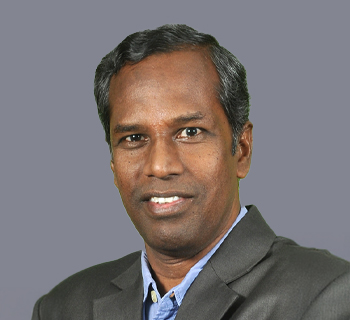
| 1 | Head of the Department | Dr. Y Chakrapani | Professor & HOD of ECE |
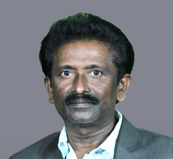
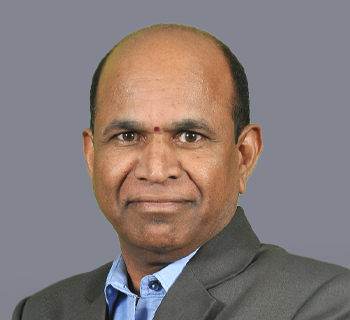
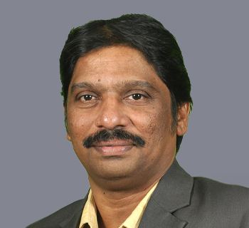
| 2 | Department Faculty | Dr. P. Satish Kumar Prof. M. Ravikumar Mr. R. Srinivasa Rao Mr. GPV Kishore Mr. Y. Pradeep |
Professor Professor Associate Professor Associate Professor Associate Professor |
| 3 | Students | J. Parthiv Patnayak Rishi Ravi Chander Sama Dixitha S. Santosh Kumar |
IV ECE IV ECE IV ECE III ECE |
| 4 | Parents | A. Ravi Chander S. Vanaja Kumari Samala Santosh Kumar Tiruvaipati Srinivas |
Branch Manager, ACE Engineering Academy, Hyderabad HR Manager in SSL Company, Hyderabad Mechanical & Electrical Technician, RCI Balapur, Hyderabad Accounts Manager, Tara Tours and Travels, Alwal, Hyderabad |
| 5 | Alumni | Deveanlla Bala Aditya P. Sai Venkata Ramana Nikhil Chakka M. Sri Harshvardhan Reddy M. Yeshawanth Reddy Hanna Grace T |
Junior Engineer, Nucleonix, Hyderabad System Engineer, TCS, Hyderabad Software Engineer, Principal Global Services Genpact, Hyderabad Accenture, Hyderabad R&D Engineer, Hyundai R&D, Hyderabad |
| 6 | Professional Bodies Member | Prof. A. Ravi Kumar Dr. V. Rama Rao |
IETE Fellow, Life Member of IE, BMESI, Retd Chairman of IETE, Hyderabad IETE Member, Life Member and Member of Technical Programmes & Publications Sub-Committee, IETE, Hyderabad |
| 7 | Industry Expert | Dr. M. Chakravarty Sampath Kumar Bathini Smt. G. Jalaja Dr. Bellamkonda Saidulu |
Scientist G, Group Director Antenna Wing, DLRL, Hyderabad Senior Software Engineer, AMD Senior Manager, SED Division, ECIL, Hyderabad Analog & Mixed Signal IC Designer, Cyient Ltd, Hyderabad |
| 8 | Employers | Mr. J.A. Narendra A. Satish Kumar Mr. A. Srikanth Reddy |
MD, Multitech Systems, Hyderabad MD, Surya Tech Solutions, Hyderabad Project Manager, CynoHub, Hyderabad |
Placements Highlights – 2021 – 25
72
Campus Interviews Conducted
9
Programs Available for the Students
46.38L
Highest Package 46.38LPA in Amazon
434
Successful Campus Placements
Our Tap Recuiters


Roll Of Honour

DUVVALA SRIKANTH
R : No : 19AG1A0433
BATCH : 2021-2025

PALLE VARSHA
R : No : 19AG1A0433
BATCH : 2020-2024

MUPPARTHY AARTHI
R : No : 19AG1A0433
BATCH : 2019-2023

KAREDLA BHAVANI
R : No : 18AG1A0483
BATCH : 2018-2022

VADDHIPARTHY S V S L N SURYA SUHAS
R : No : 16AG1A0449
BATCH : 2016-2020

MAHADEVUNI NAGARANI
R : No : 15AG1A0426
BATCH : 2015-2019

DONGARI HARIKA
R : No : 14AG1A0401
BATCH : 2014-2018

SANAGALA NEHA REDDY
R : No : 13AG1A04E8
BATCH : 2013-2017

YEDULLA SAITEJASWINI
R : No : 12AG1A04H8
BATCH : 2012-2016

MADUKU HARIKA RAO
R : No : 11AG1A0464
BATCH : 2011-2015
Syllabus
REGULATION R25
REGULATION R24
REGULATION R22
Events and Activities
Placements
| S.No | Roll ⬍ | Name ⬍ | Branch ⬍ | Company ⬍ | Role ⬍ | Package ⬍ | Year ⬍ |
|---|